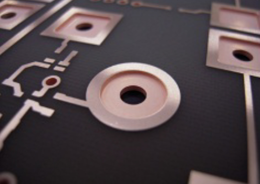
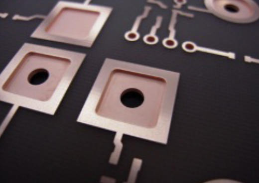
Cavity Board
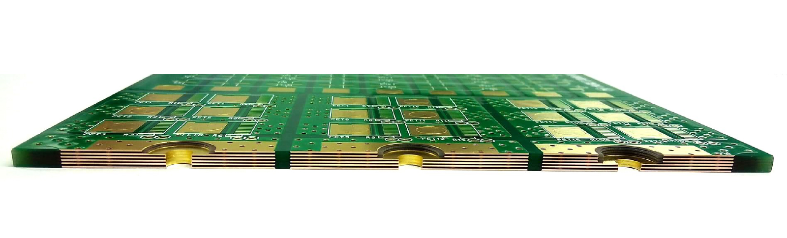
It is possible to contact Inner layer directly from the surface with Cavity structure.
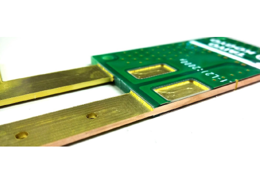
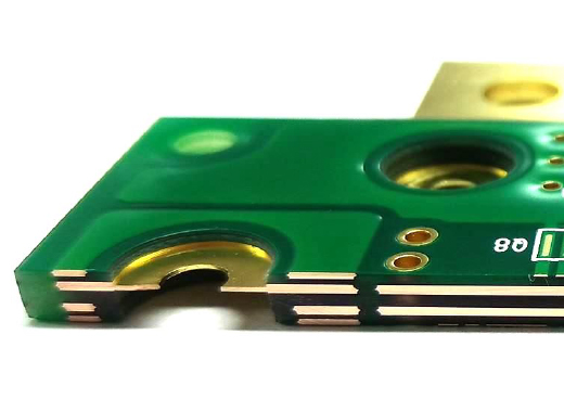
It is also possible to expose only copper in inner layers (more than 800um(22.8oz)) applying both sides cavity structure.
Features of Cavity structure
- It is possible to expose any Inner layers if thick copper is used for Inner layer of multiple layer PCB.
- Designer obtain freedom of design by selecting cavity shape and depth.
- It is possible to position screw head inside of PCB.
Specification
| Others |
|---|